Methods and tools for in-system debugging of ERA
ABSTRACT
FPGA offers a competitive solution to traditional ASIC development by reducing costs and shortening time of in-system debugging and prototyping. The core objective of this document is to design an appropriate methodological approach for In-system debugging of ERA, an Embedded Reconfigurable Architecture. A comprehensive evaluation of debugging tools and applicable methods are presented. Several tools will be evaluated for iterative debugging using a principle of growing core applied for the fault types and modes. The outcomes of the research are debugging method for the ERA based on Altera FPGA as well as analysis of efficiency of proposed methodology.
INTRODUCTION
Debugging plays a major role in increasing the performance of the processor by eliminating or by rectification of bugs. The coverage of faults (C = f(debugging, λ, RdN)) increase, the processor quality of performance and its life span increases. Debugging is introduced in the life cycle of a processor not only to give specific standard but also to improve the processor performance and efficiency in reliability aspects. To overcome the difficult challenges in debugging a system it is beneficial to choose appropriate tools and methods, to know about possible fault types there are and applicable tests.
Q α 1/λ α C (where c is fault coverage and λ is poisson failure rate).
A comprehensive evaluation of debugging tools and applicable methods are presented. Different areas like types of faults, fault injection methods and observations on applicable tools are formatted under this topic according to the ERA, an Embedded Reconfigurable Architecture environment.
PROCESSOR ARCHITECTURE:
The processor consists of two main parts: one is the control unit and the other is data path components. The data path components consist of the temporary executed data storage and functional units such as arithmetic and logical units. The instructions to be executed are fetched from the external memory into the instruction register and are decoded by the control unit (CU), which is also responsible for managing the execution of each instruction. Operands for each instruction being executed are fetched from the register file into the Arithmetic Unit (AU) and Logic Unit (LU) for operation. The processed output bits or data from AU and LU are directed to the external memory through the data bus or is written back to the Register file (for temporary). Figure9 shows that AU and LU are separated to simplified design principles. This separation gives support to debug the processor and to show fault tolerance scheme.
![Figure 9 the Architecture of the Fault Tolerance ONBASS CPU [1]](https://www.ivoryresearch.com/wp-content/uploads/2013/04/daniel-sasank-1.gif)
Figure 9 the Architecture of the Fault Tolerance ONBASS CPU [1]
The ONBASS CPU executes the three fundamental processes for instruction processing and fault tolerance. Where process P1 and P2 are involved with fault checking and recovery of malfunction (permanent or temporary) respectively. P1 is initialised at the instruction level itself i.e.., instruction execution. P2 is required and initiated when fault has been detected in instruction execution, but it is necessary that the pre-modified state is stored at the initial stage of execution of every instruction. Error detection and error recovery processes operate concurrently. Figure9 shows the three core processes of fault tolerance. The hardware for the data manipulating process P3 is marked green and error checking process P1 is marked yellow. When the data bits are written into the Register File, the checking information is generated and this information is used to check conditions of stored data bits when data bits are read out from the Register File. The check detects faults of operands before the Arithmetic Unit and Logical Unit operations. In this fault tolerant architecture in order to recovery process P2 an extra Register Buffer Rbuf (R*) is introduced, which is marked in red. When a fault is detected during instruction execution, it allows the CPU to restore the initial state (original data) before the execution of the instruction. This enables the instruction to be repeated so as to tolerate the malfunctions within the instruction level. The extra Register Rbuf (R*), the checking schemes and the instruction reversible control unit (CU) are combined to implement execution of the P1 and P2 processes without any perceptible time delay [2] [3]. To test P2 and P3 we must know about areas like types of faults and their impact on the processor at the time of recovery.
TYPES OF FAULTS, COVERAGE:
![Table: Classification of faults and their impact [6]](https://www.ivoryresearch.com/wp-content/uploads/2013/04/daniel-sasank-2.gif)
Table: Classification of faults and their impact [6]
The classification of faults is based on duration (latency), which guides reasonably. The approach to tolerating a fault depends on its duration. Tolerating a permanent fault requires the facility to avoid using the faulty component, possibly by using a fault-free replica of that component or element. Tolerating a transient fault requires no such self-repair because the fault will not persist. Fault tolerance schemes tend to treat intermittent faults as either transients or permanents, depending on how often they recur, although there are a few schemes designed specifically for tolerating intermittent faults. Studies have shown that transient faults occur far more often than permanent ones and are also much harder to detect. Finally, intermittent faults, which are caused by unstable hardware or varying hardware states, either stay in the active state or the sleep state when a computer system is running. These faults are repaired by replacement or redesign [4] [5].
The Embedded Reconfigurable Architecture implements the three fundamental processes: (P1) checking, (P2) recovery preparation and (P3) recovery. So it is important to know about types of faults to observe P2 and P3 schemes. Here in the table HW (I), HW (dT) and HW (dS) are hardware triple. HW (I) means that the extra information bit is generated by hardware, HW (dT) means that the time latency is almost negligible in comparison with the performed function (dT<<T function). HW (dS) means that hardware overheads involved in fault elimination are negligible with the total structure of unit. In order to tolerate hardware faults such as Byzantine faults, more than two copies of hardware is required. But up to now there are no representative statics that characterise the practical distribution of faults for computer systems. The distribution of faults depends on the practical environment such as vibration and radiation in aerospace applications [6].
FAULT INJECTION METHODS:
Fault tolerance scheme can be observed or verified much faster through fault injection experiments. Combining fault injecting methods with in-system debugging techniques gives benefits which result in identifying system components whose failure rate is most likely to occur at the time of system crash. In such practical attempts various faults are injected either into a simulation model of the target device or a hardware prototype and software of the system to observe the behaviour of the fault and to classify it. Parameters for these experiments are included with the probability that a fault will cause an error and the probability that a system will perform successful recovery (i.e. called coverage factor). There are two basic fault injecting techniques which were taken into account for comparison:
- Hardware (direct, indirect)
- Software (compilation, runtime)
![Table: Comparison of different Fault Injection methods [7]](https://www.ivoryresearch.com/wp-content/uploads/2013/04/daniel-sasank-3.gif)
Table: Comparison of different Fault Injection methods [7]
From the above table it is known that (SWIFI) software injection during runtime means:
- Errors are injected into source code or assembly code to emulate the effect on hardware (permanent or transient) and software faults.
- To inject these faults triggering can be allowed into circuit (software triggering, hardware triggering) during runtime.
Advantages:
- Easy to access, due to minor changes in code during runtime.
- overcomes some of the problems with physical fault injection, such as repeatability and controllability.
- provides best accessibility to control internal nodes in system.
EVALUATION OF TOOLS:
The following tools are for Altera based prototype boards. The traditional methods which Altera chips offer for in-system debugging at-speed of prototype board are:(i) Signal Probe (ii) Signal Tap-II Embedded Logic Analyzer (iii) External Logic Analyzer
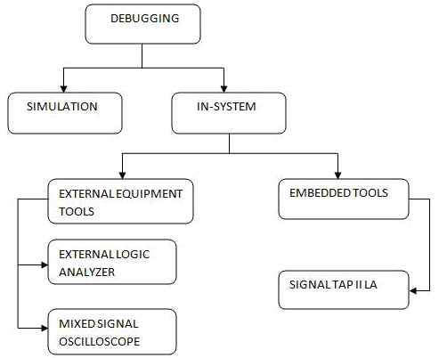
Fig: classification of debugging tools
Signal-Probe: This is a debugging technique in which external pattern generator executes the logic and a logic analyzer to analyse the output waveforms during runtime. The signal probe gives opportunity to read or tap the internal signals during runtime in the process to debug the logic design or microprocessor. In this method by driving any internal signal manually within the design specifications can allow the process of debugging more efficiently. The In-system source and probe editor in the Quartus II software extends the capability of verification tools, which allows controlling any internal signal and providing a complete dynamic debugging environment easily. Apart from providing a powerful debugging environment this method is useful to generate events in the environment that influence the behaviour and request response signals from the device [8].
Signal Tap-II Embedded Logic Analyzer: Embedded Logic Analyser is generally provided by the FPGA vendors itself. Debugging with Signal Tap II Embedded Logic Analyser gives opportunity to examine the behaviour of internal signals. There is no need to use extra I/O pins to test and analyse the device running at full-speed. The Quartus II software is included with this logic analyser free of charge. The designer is allowed to debug the design by probing the state of the internal signals in the design without the use of external equipment and physical probes. Higher accuracy and improvement in fault detection ability is achieved by defining custom trigger-condition logic in to the design. The Signal Tap II Embedded Logic Analyser needs no changes to the actual design file to capture the state of the internal nodes or I/O pins in the design. One of the great benefits is that each and every captured signal data is easily stored in the device memory to read and analyse the data [9].
External Logic Analyser: The Quartus II Logic Analyzer Interface (LAI) allows any traditional external logic analyser with a minimal number of I/O pins to examine and analyse the behaviour of internal signals while processor design is running at full speed on FPGA integrated device. The LAI gives opportunity to connect a large set of internal device signals to a small number of output pins. Analysis can be made through connecting these output pins to an external logic analyser for debugging purposes. In the Quartus II LAI, the internal signals are grouped together, distributed to a user-configurable multiplexer, and then output to available I/O pins of the device. Instead of having a one-to-one connection between internal signals and output pins, the Quartus II LAI enables designer to map several internal signals to a smaller number of output pins. The exact number of internal signals that can map to an output pin varies based on the multiplexer settings in the Quartus II LAI [10].
OBSERVATIONS:
- Signal probe and external logic analyzer needs additional IO pins. Signal Tap II does not require any additional pins.
- Both Signal Tap II and External Analyser require an active JTAG connectivity to a host running the Quartus II software. Signal Probe does not require a host for debugging purpose.
- External Logic Analyser gives much capability and visibility where signal Tap II offers triggering capabilities that are comparable to basic logic analysers.
- The External Logic Analyser via LAI has greater buffer capabilities to store more captured data than Embedded Logic Analyser. There is no concept of data capturing or storage in Signal Probe.
- Signal Probe attaches incrementally routed signals to previously reserved pins, requiring very small recompilation time to make changes to source signal selections. Both Signal Tap II and External Analysers take advantage of incremental compilation to refit their own design partitions to decrease recompilation time.
- External Logic Analyser adds minimum logic to the actual design with the usage of few device resources.
- External Logic Analyser provides better access to timing mode and enabling to debug combines streams of data.
- Signal Tap II Analyser acquires data at speeds over 200 MHz’s. Same speed is acquired with external logic analyser, but signal integrity issues may apply a limit.
- Embedded Logic Analyser is completely internal as it is available with the Altera Device. No external equipment is required other than a JTAG connection.
- Signal Tap II and External analysers provides good resource management in debugging a system.
- Embedded logic analyser is best in terms of cost, speed and time. Signal probe and External Logic Analyser need manually high effort but provide much fault detection ability.
ANALYSIS:
Each and every tool has advantages and disadvantages, as well as its own procedure and method in debugging. The following table gives an idea to differentiate:
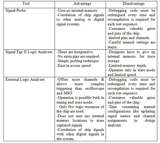
Fig: Advantages and Disadvantages of available tools
Even though it is hard manually to debug with External Logic Analyzer, designers can acquire fast boundaries with the industry’s highest acquisition speed. Support packages tuned to specific applications make it easier for designers to probe, acquire, decode, analyse and validate the performance of microprocessor, FPGA or memory design. For this reason External LA’s are suitable for any type of test environment [11].
APPROACH:
Implementation of chosen tools and method must be applied by using “principle of growing core”. To implement the test pattern both debugging and fault injection techniques must be taken into account. Injecting a known fault into the prototype board and monitoring it manually through Quartus software gives much efficiency and adaptable results. These known faults or fault injections are done before in-system debugging is started. Software injection during run time is an indirect injection method which is apt for ERA environment because code level changes are easy to modify and it takes less time to recover.
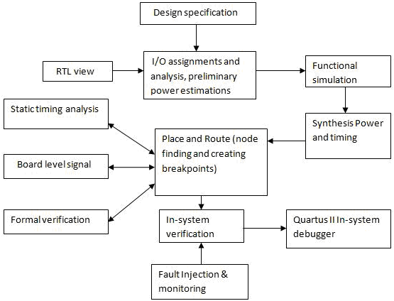
Fig: Predicted Design Flow with Fault Injection
It is easy for in-system debugging as we already know the type of fault that was injected in to processor. For debugging purposes External Logic Analyser is chosen because designers can acquire fast boundaries with the industry’s highest acquisition speed, support packages tuned to specific applications make it easier for designer to probe, acquire, decode, analyse and validate the performance of microprocessor.
Proper set up during the in-system debugging phase and application of these tools and methods yields maximum coverage as introducing a known fault by using software injection during runtime method and debugging it with external tool suits ERA environment. This proposed method will save most time during the debugging phase and simplify the process by reducing complexity. The evaluated tools and methods have their own advantages and disadvantages, but the introduction of fault injecting-and-debugging method is more responsive and appealing in nature when it is considered for a Fault-Tolerance processors. The ability to associate internal FPGA signal activity by this method to board-level signals represents total insight of embedded design and avoids unnecessary delays that were caused in finding a bug.
CONCLUSION:
A comprehensive evaluation of debugging tools and methods is presented for in-system debugging of Embedded Reconfigurable Architecture which is embedded with Altera FPGA. These tools and methods are chosen by taking fault types and modes in to account, in accordance with the ERA environment. The evaluation specifies that external logic analyser is an appropriate tool for debugging and the introduction of Software Implemented Fault Injection method for injecting and monitoring known faults into the processor will result in total coverage. This fault-injection and detection method eliminates the bottle neck conditions that occur in debugging the processor. The behaviour of the proposed tools and methods practicality is future work and yet to be proved.
REFERENCES:
[1] http://www.wrtp-rts.proceedings2009.imcsit.org/pliks/192.pdf Accessed on 21st April 2010
[2]http://www.londonmet.ac.uk/fms/MRSite/acad/foc/research/seminars/09-10/FT-NoC-Aero-Apps-IMCSIT-2009.pdf Accessed on 21st April 2010
[3]ON-Board Active Safety System, Project, Active system safety implementation: hardware design, development and analysis, ONBASS Project, 2007.
[4]J. A. Clark and D. K. Pradhan, Fault Injection A Method For Validating Computer-System Dependability, in IEEE Computer, Vol. 28, No. 6, June 1995, pp. 47-56.
[5]P. M. Wells, K. Chakraborty, and G. S. Sohi, Adapting to Intermittent Faults in Multicore Systems, In Proceedings of the Thirteenth International Conference on architectural Support for Programming Languages and Operating Systems, doi:10.1145/1346281.1346314, Mar. 2008
[6]Thomas Kaegi-Trachsel, Igor Schagaev, Juerg Gutknecht, system software support for possible hardware deficiency, On-Bass project, 30 Dec 2009
[7] Israel Koren and C.Mani Krishna, Fault Tolerant systems, Morgan Kaufmann publication, ISBN 0-12088525-5, 2007.
[8] Design Debugging Using In-System Sources & Probes, Quartus II 9.1 Handbook, Altera Corporation, Volume 3, 2009 <http://www.altera.com/literature/hb/qts/qts_qii53021.pdf> > accessed on 8th March 2010
[9] Design Debugging Using the SignalTap II Embedded Logic Analyzer, Quartus II 9.1 Handbook, Volume 3, 2009 <http://www.altera.com/literature/hb/qts/qts_qii53009.pdf> accessed on 8th March 2010
[10] In-System Debugging Using External Logic Analyzers, Quartus II 9.1 Handbook, Altera Corporation, Volume 3, 2009 <http://www.altera.com/literature/hb/qts/qts_qii53016.pdf> accessed on 9th March 2010
[11] <http://www.altera.com/literature/lit-cyc2.jsp> accessed on 8th March 2010