The design and creation of a precises temperature control system.
Chapter 1
INTRODUCTION
The following project deals with designing and creating a precise temperature control system for stabilising the operational temperature for a variety of operations ranging from laser drivers to chemical reactions. To this end, a hybrid proportional-integral control feedback circuit would be designed, tested and constructed. The system will allow the user to regulate a thermal load at a chosen temperature.
Laser driver circuits consume a lot of power and produce large amounts of heat. Their performance and optical output declines as they get hotter. Most commercial temperature controllers can provide stability to a precision of less than 0.0020 C. Although acquiring industry grade precision is out of the scope of this project, we will construct a system to provide stable temperature control and reasonable levels of precision.
Chapter 2
Devices used
Most of the devices used in the construction were basic analog devices. The LM 353 is a DIP op amp and forms one of the major building blocks in the entire circuit. It is used in several configurations – as a buffer, as an integrator and as a differential amplifier. Two Darlington transistors were used, one NPN and one PNP. The device used for cooling was a thermoelectric cooler, also known as a Peltier. The component used was a Supercool PE 063-08-15 from RS electronics. Some of its specifications from the data sheets (relevant to our discussion) are as follows:
Max current: 2.2A
Max voltage: 7.6V
Maximum Temperature: 800 C
Peltiers are thermocouples that develop a temperature difference between the two metals when a voltage is applied. One side absorbs heat, and the other emits it. Reversing the voltage would cause the opposite effect[1].
The Peltier that was used had an attached thermistor that would measure the change in temperature as a function of resistance. This thermistor was an NTC RS 151-237. It had a negative temperature coefficient, i.e. its resistance varied inversely with temperature.
| Reference Point | |
Temperature oC | 25oC |
Resistance (ohm) | 10,000 |
Tolerance +- % | 0.88 |
The resistance at different temperatures is calculated using the following equation:
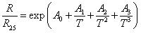
… where R25 is the resistance at reference temperature, T is the temperature whose resistance is to be calculated, and A0, A1, A2, A3 are constants provided by the manufacturer.
Or[2],
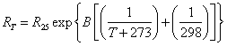
My device constants as from the data sheets are as follows:
| B value | ~3902 |
| A0 | -1.409E+01 |
| A1 | 4.345E+03 |
| A2 | 3.054E+03 |
| A3 | -1.376E+07 |
As is characteristic of all thermistors, the resistance of my component too did not vary linearly with temperature.
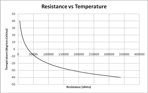
Figure 1. RvsT characteristics illustrating non linearity.
Chapter 3.
Before we dig into the design of the project, we define the condition for stability in an op amp feedback circuit:
“The criterion for stability against oscillation for a feedback amplifier is that its open loop phase shift must be less than 1800 at the frequency at which the loop gain is unity[3].”
—-(Horowitz) (Hill, 1989)[2nd Ed]
Design.
3.1. Temperature Detection.
The very first part of my design was creating a system to measure temperature. The non linearity of the thermistor, as illustrated in figure 1, Ch.2, would make it difficult to implement it effectively in any temperature detection system. We could linearise this curve in two ways: resistance mode or voltage mode[2]. In resistance mode, the thermistor is connected in parallel with another resistor. Choosing a resistor with a value close to the reference point would linearise the curve around that temperature.
Figure 2. Effect of resistance mode linearization (2)
However, we need a temperature reading outputted in voltage (for reasons discussed later). To this end, I had to design a voltage divider circuit which would output a voltage that would vary linearly with temperature, i.e. use voltage mode.
3.1.1. Voltage Divider design.
The very first thing that needed to be designed was the other value of resistance in the divider as this value would linearise my curve across the desired range. This is done using [4]:
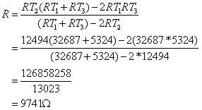
Where RT1, RT2, and RT3 are the resistances at low, middle and high points of my temperature range, in this case 0, 20, and 40 degrees celcius.
For my reference voltage, I used a 1.5V AA battery. This was chosen based on data sheets of other temperature controllers for lasers.
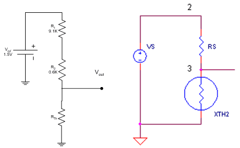
Figure 4. Completed voltage divider circuit & Figure 3. SPICE simulation diagram
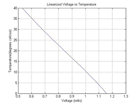
Figure 5. There is now a linear response to temperature change
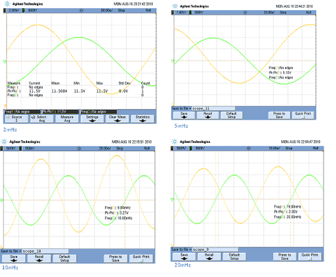
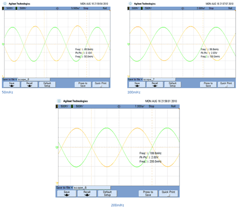
3.1.2. Frequency Response
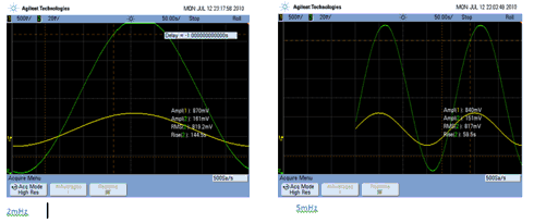
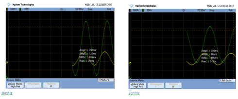
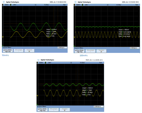
In order to design a stable feedback loop, we now have to find the frequency response of this system. I hooked up a waveform generator to my voltage divider and sent a 1V amplitude sine wave, and measured the output on a CRO at different frequencies. This data was then put together on a couple of Bode plots as shown below1.
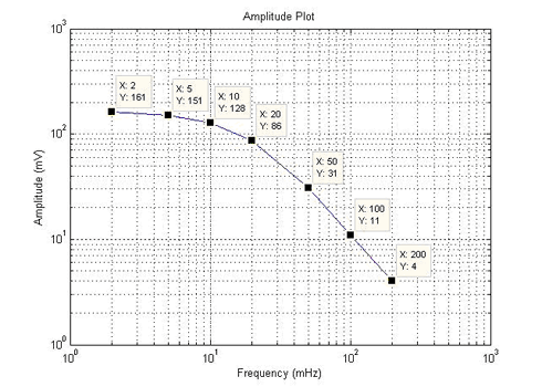
Figure 6. Amplitude of the output wave at different
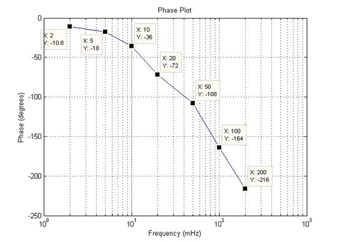
Figure 7. Phase difference between input and output wave at different frequencies
3.2. Proportional Control
A proportional controller acts to supply power proportional to the difference in the current state and the setpoint[5].
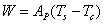
… where Ap is the gain of the proportional controller, and Ts and Tc are the setpoint and current temperatures respectively.
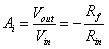
In the case of my design, I used a subtractor or a differential amplifier for this purpose.
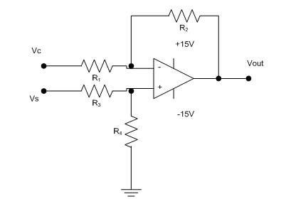
Figure 8. Standard differential amplifier circuit.
… where,
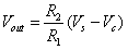
… when

Based on my Bode plots (figures 6 and 7), I had to design a proportional gain control of 1 or less than 1 at the point where there was a phase shift of 1800 and also accounting for a phase margin of ~450 to have a stable feedback loop without oscillations. This point is at where freq = 50mHz and phase difference is -1080. Since my input was 1V and output (at 50mHz) was 31mV, my gain had to be 30. My completed differential amplifier circuit was as follows:
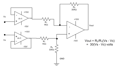
Figure 9. Completed design for differential amplifier.
Since both my inputs would have an impedance that would vary with temperature, input buffers were added to remove the need for impedance matching[6]. These buffers are just simple op amp follower circuits with gain =1.
There is a slight constant difference in the final and setpoint temperature, to ensure voltage is being supplied to continue regulating the temperature. Increasing the gain would make the response time shorter and the final regulated temperature more precise, but beyond a point the system would become unstable and oscillate.
3.3. Integral Control
An integral controller controls the voltage based on the time integral of the error. The output of my integral controller would supply a voltage proportional to the sum of recent errors in the desired and current temperature with some gain I.
 (7)
(7)
For my design I used a typical integrator amplifier with one modification (for getting the required frequency response, which will be discussed later). The integrator also eliminates the steady state error associated with systems having only proportional control.
![Figure 10. Typical Integrator circuit. Image from [8]](https://www.ivoryresearch.com/wp-content/uploads/2013/04/ronald-kovacs-fig-161.gif)
Figure 10. Typical Integrator circuit. Image from [8]
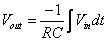
Or
When this circuit is switched on, i.e. a voltage is applied, the capacitor being uncharged, acts as a short and there’s a gain of less than 1. As the capacitor charges, the gain increases exponentially to infinity until the circuit rails[6].The gain of an integrator amplifier at higher frequencies is zero, and it increases exponentially at lower frequencies. At DC or zero frequency, its gain is infinite.
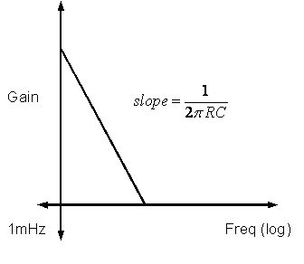
Figure 11. Typical gain vs frequency plot of an integrator amplifier
However, the integrator circuit would introduce a 900 phase shift in my signal. Therefore, to satisfy the stability criterion, my system would now have to have a gain of 1 or less at a point in frequency that has a phase shift of:
180 – (90+45) degrees
… where 45 is accounting for a phase margin (see section 2.2)
<=450
This point is at where frequency is at 10mHz and there’s a phase shift of 360 (see fig 6 and 7). Therefore, my integrator amplifier would have to be modified to provide a gain of 1 at frequencies higher than 10mHz, and my graph from figure 9 would have to look like:
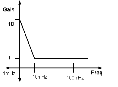
Figure 12. Required frequency response
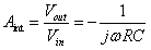
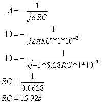
We know that the capacitor acts as a short at higher frequencies giving a gain of zero. Therefore, to get a gain of 1, there would have to be a resistor in series with the capacitor having an equal value as the one forming the RC pair. Basically, at higher frequencies, the circuit would have to act as an inverting amplifier:
![Figure 13. Typical inverting amplifier. Image from [9]](https://www.ivoryresearch.com/wp-content/uploads/2013/04/ronald-kovacs-fig-211.gif)
Figure 13. Typical inverting amplifier. Image from [9]
Where,
To find the exact RC values, we just substitute the required gain and frequencies in eqn (1):
I now have a completed design for my integral controller system.
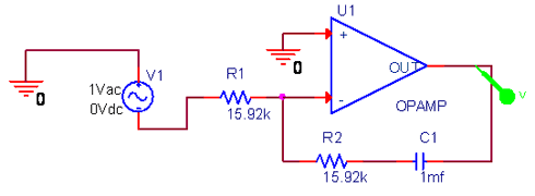
Figure 14. SPICE schematic showing ideal albeit theoretical values.
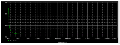
Figure 16. SPICE simulation results for frequency response of integral controller with linear X axis
Figure 15. SPICE simulation for frequency response with logarithmic X axis
3.4. Final Gain stage
Since the output current of my op amps would be in the range of a few millivolts, there would be a need to amplify this signal to drive my TEC which could need up to 1-2 amps to reach the desired temperature. Ideally, a power amplifier would be suitable for this purpose, but due to logistical and time constraints, we had to design a substitute.
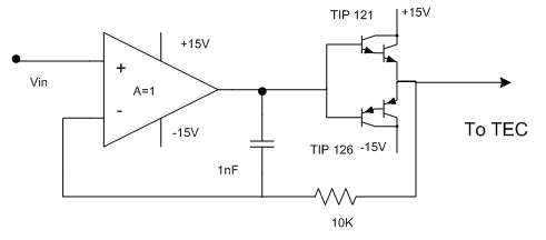
Figure 17. Emitter follower amplifier design.
In the above design, two Darlingtons are connected in a complementary emitter follower circuit to a voltage follower with a small capacitor in its feedback loop. At high frequencies, the capacitor is shorted and the circuit simply follows its input. At lower frequencies the loop is opened and the emitter amplifier circuit provides a current gain. Since there needs to be a bilateral current supply, two transistors are used. When a positive signal is applied, the TIP 121 which is an NPN, goes into forward bias and the TIP 126 is cutoff. At negative voltage, the TIP 121 is cutoff, and the 126 provides constant current.
3.5. Setpoint.
Finally, all that remains is telling the control loop what my temperature should be. Since my setpoint circuit had to be a variable function of my reference voltage Vref I had to design another voltage divider circuit, this time with a potentiometer.
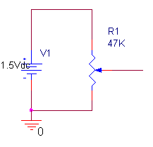
Figure 18. Setpoint design.
3.6. Completed circuit.
The entire circuit design is now complete. Resistors R1 and R2 provide a resistance total of 9.7K and R3 and R4 (1K and 30K respectively) give my differential amplifier a gain of 30 as required. I used LM 353’s for all my op amp configurations. For the capacitors in my integrator, I had to use plastic, as ceramic capacitors can’t handle reverse voltage. Two of them in parallel give me a combined 0.5mF. The two matched resistors, each 3.2MΩ give me an RC time constant of 16, and provide equal output at higher frequencies. Two Darlington NPN and PNP transistors were connected in an emitter follower configuration to provide current amplification. The thermoelectric cooler, i.e. the Peltier is thermally coupled with the thermistor in the first voltage divider to measure temperature changes and this closes the loop.
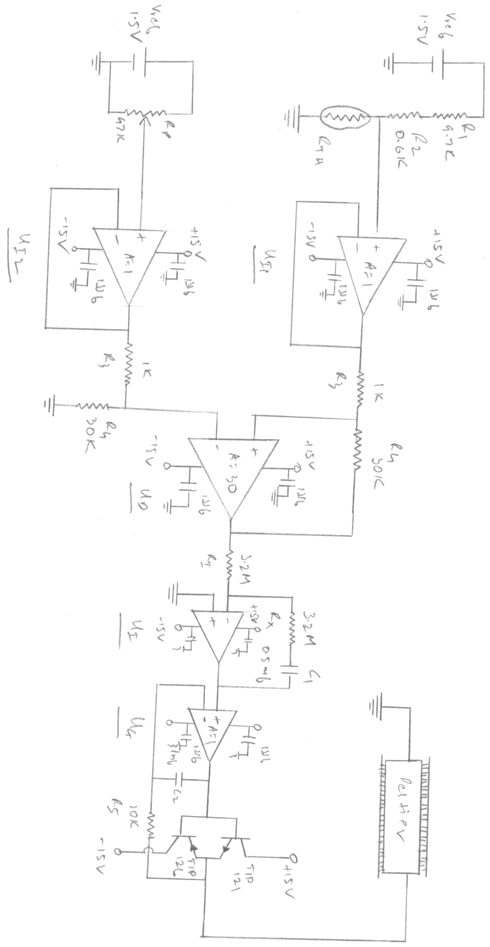
Figure 19. Completed circuit diagram with all components and values
Chapter 4
Construction and Working
4.1. Construction
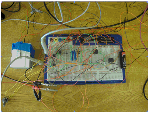
Figure 20. Fully constructed and operational circuit.
The circuit is now ready. A standard AA battery with 1.5V provides reference voltage to both my voltage dividers. On the left you can see the Peltier which is attached to a heatsink to dissipate heat. The thermistor is thermally attached to the Peltier to measure temperature. Two CRO probes measure the voltage level of my desired and current temperatures. The transistors are fitted with heatsinks as they were getting too hot to take more than a couple of readings at a stretch. Adjusting the potentiometer would specify the required temperature.
4.2. Working.
When the power is turned on, the thermistor divider reads a voltage at room temperature. The output of UI1 is the same as this voltage. If the potentiometer is adjusted to a higher voltage than this, UI2 follows as well. The output of UD is this difference multiplied by a factor of 30 in voltage. This voltage drives the integrator UI to provide a voltage that is amplified by the TIP 121, while the TIP 126 is in cutoff. A positive current is sent to the Peltier, which causes it to cool. As its temperature decreases, the voltage across the thermistor divider increases. The integrator measures the changing error and regulates its output to provide a constant temperature at the setpoint.
Chapter 5.
Testing and Troubleshooting.
5.1. Testing.
Testing for the circuit was carried out in stages.
- The voltage dividers were first tested, which was easy enough to verify, as the theoretical values could be calculated and compared to the actual values with a multimeter or a CRO.
- The input buffers were then tested to make sure the power rails were being supplied with full voltage. Having checked that, their output was measured with a multimeter to make sure it was the same as the respective voltage dividers.
- I then had to test the differential amplifier. To do this, I measured the current temperature and selected a setpoint and measured the output of the op amp. Here are some readings I measured:
UI1 (volts) | UI2 (volts) | Difference (volts) | Theoretical Value (V) | Measured Value (V) |
0.799 | 0.655 | -0.145 | -4.35 | -3.9 |
0.799 | 0.967 | 0.168 | 5.04 | 4.7 |
0.8 | 1.21 | 0.41 | 12.3 | 11.4 |
There was some error here, but it could be due to a slight mismatch in resistance or slight offset voltage from the op amp. The LM 353 has an offset voltage of 10mV. With a gain of 30, this amplifies to 300mV, so that could explain some of the error.
- Testing the integrator was a little tricky, as the output voltage would rail regardless of the input. After the integrator was constructed, and its supply rails and connections tested, I hooked up a waveform generator and sent a 1V amplitude signal at different frequencies ranging from 2mHz to 200mHz to get its frequency response. The gain and phase shift data was then put together on a Bode plot.
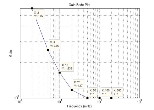
Figure 21. Bode plot of gain.
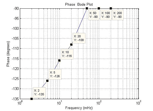
Figure 22. Bode plot of phase difference.
As you can see, the gain plot in figure 18 is quite similar to the SPICE simulation graphs from figures 12 and 13. The integrator provides unity gain at higher frequencies and an exponentially increasing gain at lower frequencies as expected.
5.2. Troubleshooting
The circuit was constructed on a breadboard, and as is typical with breadboards, there were several hiccups in getting it working right. Listed below are some of them:
- After constructing the entire circuit sans the emitter follower, my AA battery exploded. Cause: The voltage dividers were getting voltage from both the battery and the 15V supply rails for the op amps due to some wires crossing. Tweaking the potentiometer all the way caused the battery to explode.
- The system was heating and regulating the temperature around the setpoint, but wasn’t cooling. Cause: The TIP 126 was dead. This was probably because of overheating from previous readings. Replacing the transistor and attaching heatsinks to each of them fixed this problem.
- The temperature was oscillating about its setpoint. Cause: The power supply used was current limited, it only had a maximum output of 200mA. Supplying voltage to the emitter follower amplifier from another power supply gave a steadier output.
Chapter 6
Results
For the final testing of the entire system, two CRO probes were attached to each voltage divider. The setpoint and current temperature were outputted in voltage on the CRO. Adjusting the setpoint to a particular value, and switching on the power to the op amps gave the following results:
6.1. Cooling
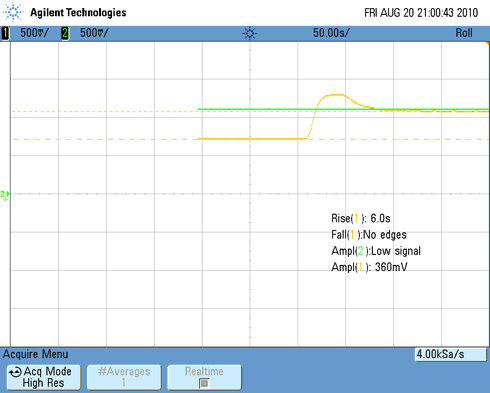
Figure 23. Completed system response, testing cooling.
The yellow graph represents the temperature on the Peltier, and the green graph is the setpoint. The CRO is set at 50 seconds per division. On switching on the power, the voltage across the thermistor divider jumps up sharply after a difference in voltages is detected. There is a small overshoot after which the temperature stabilises at the setpoint with a small steady state error.
Room temperature: 250 C => 0.76 V
Setpoint: 00 C => 1.12V
Rise time: 6 seconds
Total time to stabilization: 75 seconds.
Error: 4-5mV => ~0.40 C
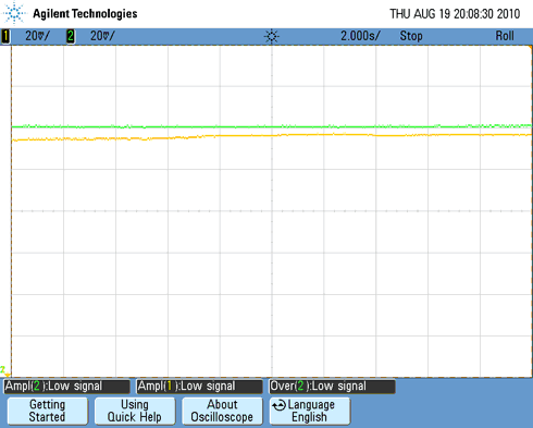
Figure 24. CRO output of regulated temperature zoomed in to illustrate error.
In the above CRO output, each channel is set at 20mV/div. The temperature of my Peltier is just a little higher than the setpoint by about 4-5mV, which corresponds to about 0.35-0.40 C.
6.2. Heating.
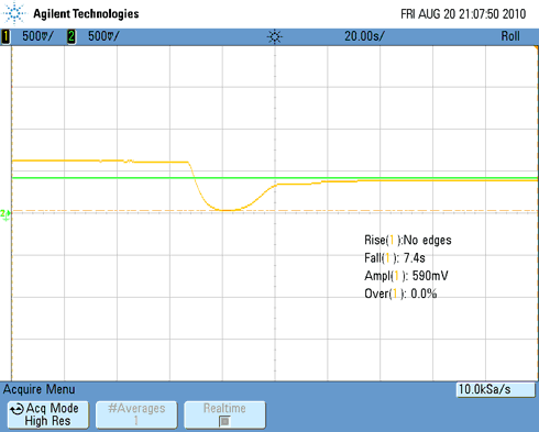
Figure 25. Heating test.
Once again, the yellow line represents the actual temperature, and the green represents the setpoint. The time division is at 20 seconds per division this time. The circuit is now told to heat the device, as the voltage of the setpoint is lower. The room temperature shows a little higher this time, probably due to latent heat from previous readings. The time to stabilisation is a little lower as the difference between the actual and setpoint values is lesser.
Room temperature: 310 C => 0.66V
Setpoint: 0.38V => 520 C
Fall time: 7.4 seconds
Time to stabilization: 70 seconds
Overshoot: 3.1%
Error: 4-5mV
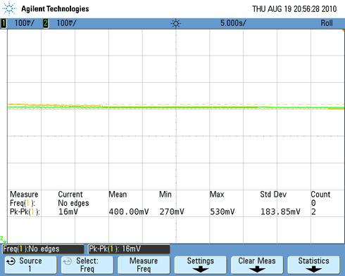
Figure 26. Temperature regulation without error.
There wasn’t always an error though. The figure above is a zoomed-in CRO reading with no error. The system was stable in this state, and had a steady voltage output.
Chapter 7
7.1. Limitations
A complementary emitter follower amplifier was used to amplify current. Due to time restrictions, there was no time to order a power amplifier which would have been a more elegant design. The transistors used in the amplifier would heat up, which made acquiring readings difficult. This also meant that the system couldn’t be left running for too long. Attaching heatsinks mitigated this problem, but only slightly. The power supplies used were also being current limited, which made it necessary to use two separate ones at the same time. The system’s response time was long, due to the frequency of operation. There was also some steady state error, which could be fixed by making some gain adjustments. Optimising the gain of the proportional controller could perhaps reduce the stabilisation time.
7.2. Conclusion
A working, operational temperature controller was designed, constructed and tested. The system consisted of a PI feedback controller to regulate the temperature with some minor error. Although most commercial temperature controllers have a higher degree of precision, for the simplicity of this design a reasonable level of precision was achieved.
Appendix A
A.1. SPICE simulation netlists:
THERM_CKT1.CIR – LINEARIZED THERMISTOR
*
* TEMPERATURE
VTEMP 10 0 PWL(0MS 0DEG 100MS 40DEG)
RD1 10 0 1MEG
*
* CURRENT SOURCE AND PARALLEL RESISTOR
IS 0 1 DC 0.1MA
RP 1 0 10000K
XTH1 1 0 10 0 NTC_10K_1
*
* VOLTAGE SOURCE AND SERIES RESISTOR
VS 2 0 DC 10
RS 2 3 9741
XTH2 3 0 10 0 NTC_10K_1
*
*
* THERMISTOR SUBCIRCUIT ************************
*
* thermistor terminals: 1,2
* temperature input+,-: 4,5
* (temperature in deg C)
*
.SUBCKT NTC_10K_1 1 2 4 5
ETHERM 1 3 VALUE={i(VSENSE)*10K*EXP(3902/(V(4,5)+273.15)-3902/(25+273.15)) }
VSENSE 3 2 DC 0
.ENDS
*
*
* ANALYSIS
.TRAN 0.1MS 100MS
* VIEW RESULTS
.PRINT TRAN V(3)
.PROBE
.END
Integrator:
*Analysis directives:
.AC LIN 1000 1mHz 200mHz
.PROBE V(alias(*)) I(alias(*)) W(alias(*)) D(alias(*)) NOISE(alias(*))
.INC “..SCHEMATIC1.net”
**** INCLUDING SCHEMATIC1.net ****
* source INT_FREQ_R
R_R1 N00274 N00163 15.92k TC=0,0
C_C1 N01706 N00235 1mf TC=0,0
E_U1 N00235 0 VALUE {LIMIT(V(0,N00163)*1E6,-15V,+15V)} _U1 0 N00163 1G
V_V1 0 N00274 DC 0Vdc AC 1Vac
R_R2 N00163 N01706 15.92k TC=0,0
**** RESUMING Int_Freq_r.cir ****
.END
A.2. MATLAB m files:
Thermistor voltage divider graph of voltage vs temperature:
r = [337240.06 315631.84 295540.64 276851.39 259458.38 243264.41 228180.07 214123.10 201017.77 188794.32 177388.46 166740.93 156797.08 147506.48 138822.57 130702.36 123106.12 115997.13 109341.43 103107.61 97266.60 91791.47 86657.29 81840.95 77321.01 73077.63 69092.35 65348.06 61828.88 58520.04 55407.83 52479.49 49723.15 47127.79 44683.13 42379.60 40208.30 38160.92 36229.73 34407.50 32687.51 31063.47 29529.53 28080.19 26710.34 25415.21 24190.32 23031.49 21934.80 20896.61 19913.47 18982.19 18099.75 17263.34 16470.31 15718.20 15004.67 14327.55 13684.80 13074.48 12494.79 11944.05 11420.65 10923.11 10450.00 10000.00 9571.87 9164.44 8776.59 8407.29 8055.56 7720.46 7401.14 7096.77 6806.58 6529.82 6265.82 6013.93 5773.52 5544.02 5324.87]; %thermistor resistance
vout = 1.5*(r./(r+9700)); %voltage divider calculation
temp = [-40:40]; %corresponding temperature range
plot(vout,temp), xlabel ‘Voltage (volts)’, ylabel ‘Temperature(degrees celcius)’,grid on;
Appendix B
CRO readings:
B.1. Frequency response of thermistor divider:
B.2. Integrator frequency response:
References
[1] http://www.heatsink-guide.com/peltier.htm
[2] http://www.maxim-ic.com/app-notes/index.mvp/id/817
[3] Paul Horowitz, Winfield Hill, 1989, 2nd Edition, The Art of Electronics, Ch. 4, page 245.
[4] http://www.ecircuitcenter.com/circuits/therm_ckt1/therm_ckt1.htm
[5] http://newton.ex.ac.uk/teaching/cdhw/Feedback/ControlTypes.html#PropCtl
[6] http://en.wikipedia.org/wiki/Instrumentation_Amplifier
[7] http://www.netrino.com/Embedded-Syst 1
[8] http://www.electronics-tutorials.ws/ 1
[9] http://www.seas.upenn.edu/~ese205/Labs06/Lab5.html